Sort yield and final test yield should, in theory, be close. Sort screens for electrical failures at the wafer level before dicing and packaging; final test screens the assembled package for functional failures at operating conditions. The gap between the two numbers represents failures introduced during assembly — die attach, wire bond, mold compound encapsulation, BGA reflow — or failures that sort missed because the test conditions at sort didn't stress the marginal devices sufficiently.
In practice, the sort-to-final-test gap at OSAT facilities is often wider than the assembly process alone can explain. When that gap widens, the diagnostic question is whether the failure modes emerging at final test were latent at sort (a sort escape), were induced during assembly (an assembly-induced failure), or are correlated with upstream fab process conditions that appear in the wafer-level data but were never systematically analyzed. This article focuses on that third category — the upstream correlation — because it is the most addressable and the most frequently overlooked.
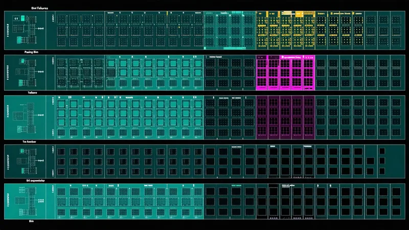
Bin Definitions and What They Actually Represent
Bin numbering conventions vary across foundries and OSAT facilities, but the general structure is consistent. Bin 1 is the passing bin — all functional devices that meet all parametric specifications at sort conditions. Higher bin numbers represent failure categories, typically structured in ascending severity of failure mode:
- Passing bins — Bin 1 is the standard pass. Some fabs define secondary passing bins (Bin 1A, Bin 1B) for devices that pass functional test but fall into different speed or power consumption grade buckets. These are binning-for-grade, not binning-for-failure.
- Parametric soft fails — Bin 5 and Bin 6 in many conventions represent devices that fail parametric specifications but pass functional logic tests. These are the most diagnostically interesting bins because the failure mode is measurable (threshold voltage out of spec, leakage current elevated) but the device still functions. They often correlate with process layer variations — threshold voltage implant dose, oxide thickness uniformity — that are visible in WAT probe data.
- Hard fails — Bin 7 and above represent devices that fail functional test — open circuits, short circuits, stuck-at faults. These are more likely to represent physical defects introduced during fab processing or, in the OSAT context, assembly damage.
The bin map is a spatial representation of this bin assignment across the wafer — each die position in the die grid carries its bin number. When you overlay the bin map on the coordinate system of the original wafer inspection data, spatial patterns in bin failures become visible. A cluster of Bin 5 failures in the upper-right quadrant of multiple wafers points toward a localized process condition; random Bin 7 distribution across the wafer surface points toward a different mechanism entirely.
STDF: The Common Data Format
Standard Test Data Format (STDF) is the industry-standard binary format for semiconductor test data, published by Teradyne and widely adopted across the test equipment ecosystem. An STDF file contains a structured sequence of records: the MIR (Master Information Record) with lot-level metadata, the SDR (Site Description Record) with test head and site configuration, PIR/PRR (Part Information / Part Results Records) for each die tested, and PTR (Parametric Test Record) for individual parametric measurements.
The die coordinates are carried in the PRR record fields X_COORD and Y_COORD, referenced to the die grid origin. The bin assignment is in HARD_BIN and SOFT_BIN fields of the PRR. This gives you everything needed to reconstruct the bin map: iterate over PRR records, extract (X_COORD, Y_COORD, HARD_BIN, SOFT_BIN), and plot against the die grid defined in the WCR (Wafer Configuration Record).
For sort-to-final-test correlation, you need the STDF file from both the sort operation (wafer-level probe, pre-dicing) and the final test operation (packaged device, post-assembly). The sort STDF carries die-level bin assignments with wafer coordinates. The final test STDF carries device-level bin assignments, but without wafer coordinates — the packaged device no longer has positional context relative to its original wafer location.
This is the core technical challenge: recovering the original die coordinates for each packaged device tested at final test. It requires a chain-of-custody traceability system that records the mapping from die coordinates at sort to package serial number or tray position at final test. Without this mapping, final test yield is an aggregate number with no spatial resolution — you know that 3.2% of devices failed final test but you can't ask whether those failures were spatially clustered on the original wafer.
Building the Sort-to-Final-Test Traceability Bridge
The traceability mapping between sort die coordinates and final test device identity is typically maintained by the assembly tracking system. The assembly operation — singulation, die attach, wire bonding — records which die from which wafer position was placed in which package position on which boat/tray/strip. The boat/tray/strip ID then carries through the assembly process into the final test handler.
In well-instrumented OSAT facilities, this mapping is available in the MES database as a die-to-package lookup table. In less-instrumented facilities — particularly those handling high-volume commodity packages — the mapping may exist only in the bonding machine log files, in a format that requires parsing to reconstruct.
Once the mapping is established, the correlation pipeline is:
- Parse sort STDF → extract (wafer_id, x_coord, y_coord, sort_bin, sort_ptrs)
- Parse final test STDF → extract (device_id, final_bin, final_ptrs)
- Join on die-to-package mapping → (wafer_id, x_coord, y_coord, sort_bin, final_bin)
- Compute bin transition matrix: for each (sort_bin, final_bin) pair, count occurrences
- Overlay final_bin on wafer coordinate grid → spatial final test bin map
The bin transition matrix is the diagnostic centerpiece. A well-behaved assembly process will show most sort Bin 1 devices staying at final Bin 1, with a small fraction escaping to final Bin 7 (hard fail) due to assembly damage. A process with a sort escape problem shows a significant population of sort Bin 1 devices transitioning to final Bin 5 or Bin 6 — functional at sort but failing parametric at final test conditions, suggesting marginal devices that passed sort only because sort conditions were less stressful.
A Scenario: Bin 5 Clustering at an Advanced Packaging Facility
An OSAT facility handling flip-chip BGA packages for a power management IC in late 2024 observed a gradual increase in final test Bin 5 (Vt out-of-spec) failures across an 8-week production window. Sort yield remained stable at 94.1%, but final test yield dropped from 92.3% to 89.7% — a 2.6 percentage point gap increase that translated directly into customer returns and expedite requests.
The initial hypothesis was assembly-induced parametric shift — BGA reflow thermal stress is known to cause threshold voltage shifts in thin-oxide devices when reflow profile temperatures exceed the upper specification limit. The reflow profile was audited and found within specification.
When the traceability mapping was used to reconstruct the spatial distribution of final Bin 5 failures on the original wafer grid, a different pattern emerged. The Bin 5 failures were not randomly distributed across the wafer — they were concentrated in a crescent-shaped zone spanning the upper-left to lower-right diagonal of wafers from two specific lots. This spatial pattern is inconsistent with assembly-induced effects, which typically produce either random spatial distribution (random assembly damage) or edge-concentrated patterns (mold compound edge stress).
The crescent pattern, when overlaid on the wafer inspection data from the photolithography layer upstream of gate oxide growth, corresponded to a reticle-field overlay shift that had been flagged — but not acted upon — in the metrology data three weeks earlier. The overlay shift had moved threshold implant dosing slightly out of spec for the affected die positions, producing devices that were marginally within sort spec but outside final test parametric spec under the more aggressive final test conditions.
Root cause: photolithography overlay drift at the foundry level, not assembly-induced parametric shift at the OSAT facility. Corrective action: foundry overlay correction and re-screening of the affected lot window. Time from initial observation to root cause: 47 minutes of analysis, 3 days of fab coordination.
Package-Level Effects and When They Are the Real Root Cause
We're not saying every sort-to-final-test gap traces to upstream fab conditions. Assembly process effects are real, and some failure modes are genuinely assembly-induced rather than wafer-level latent defects.
Mold compound stress is the most common assembly-induced parametric shift mechanism in packages with large die-to-package area ratios. Thermal expansion mismatch between the die (silicon, CTE ~3 ppm/°C) and the mold compound (epoxy, CTE ~15-20 ppm/°C) generates mechanical stress on the die surface during thermal cycling in the reflow and cure process. This stress concentrates at die corners and edges, producing a characteristic stress distribution that manifests as elevated threshold voltage (tensile stress) or reduced threshold voltage (compressive stress) depending on the MOSFET orientation relative to the stress gradient.
Assembly-induced stress failures produce a distinctive spatial signature: die-corner clustering with a roughly symmetric four-corner pattern, or edge-ring pattern in packages where the mold compound contacts the die perimeter. This pattern is different from the wafer-level signatures (quadrant asymmetry, crescent, center spot) that characterize fab-level process variation.
Wire bond integrity failures — open bonds, ball bond shear under thermal stress — produce Bin 7 hard fails, not Bin 5 parametric fails. If your yield gap is primarily Bin 7, look at the assembly process before looking at the fab data. If it's primarily Bin 5 or Bin 6 with wafer-level spatial patterning, the upstream correlation is the right place to start.
Closing the OSAT-Fab Feedback Loop
The longer-term value of bin map correlation is not just diagnosing individual excursions — it's establishing a systematic feedback channel from OSAT final test results back to the foundry's yield engineering team. Without this channel, the foundry receives no signal that a parametric shift in metrology data three weeks ago is showing up as final test yield loss at the OSAT today. The foundry's SPC system might flag the metrology excursion at the time, but if no yield impact was observed in-line, the signal is treated as a minor drift and logged without corrective action.
With the correlation data in hand, the OSAT can provide the foundry with a specific, evidence-backed report: lot window, spatial pattern, bin transition matrix, overlaid wafer inspection data, and calculated yield impact. This gives the foundry's yield team the ability to prioritize the upstream process excursion — not because their SPC chart flagged it, but because the downstream yield consequence is now quantified.
The practical barrier is data format and access. STDF files from the OSAT and KLARF or wafer map data from the foundry are rarely in the same database, and the matching key — lot ID or wafer ID — needs to be preserved through the entire supply chain handoff. Establishing that linkage, and maintaining it consistently, is the operational prerequisite for the correlation to work. It's not a complicated technical problem, but it requires deliberate coordination at the handoff point between foundry shipping and OSAT receiving.
Once the data linkage is in place, the correlation runs automatically. The analysis that took a team three days of manual spreadsheet work can complete in under an hour. The spatial patterns don't change; the time to see them does.