Every wafer map tells a story. The question is whether you can read it before the next critical layer compounds the damage.
In-line inspection tools produce KLARF files — structured defect coordinate records that capture the (x, y) centroid of every detected event on a wafer, alongside defect class, size, and layer metadata. Most fabs have been ingesting KLARF data for years. Far fewer have built a systematic practice of extracting the spatial narrative from that data: the difference between a defect distribution that is trying to tell you something about your process and one that simply reflects the background noise of a healthy fab.
This article is about that distinction — why it matters, what the canonical pattern signatures look like, and where pattern recognition breaks down even when it seems to be working.
What "Systematic" Actually Means in Defect Context
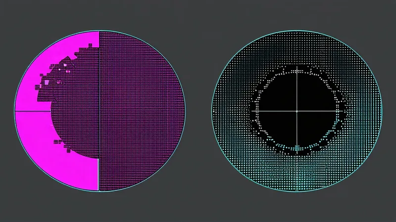
A random defect distribution follows Poisson statistics. Given a defect density D0 of, say, 0.08 cm−2 at a 5nm inspection sensitivity on a 300mm wafer with ~700 cm2 printable area, you expect roughly 56 defects — distributed with no spatial correlation to wafer geometry, process zone, or equipment position. Their spatial autocorrelation is essentially zero. Monte Carlo simulations of random D0 are indistinguishable from the distribution you see on a healthy wafer after a well-tuned etch step.
A systematic defect distribution is different in a measurable way: the spatial autocorrelation is non-zero, and the pattern of correlation maps to a physical cause within your process. "Systematic" is not a severity label — a systematic defect count can be numerically lower than a random background. What makes it systematic is the pattern, not the count. This is where inexperienced teams make a costly error: they dismiss low-D0 maps as clean because the total defect count is acceptable, while a persistent edge-ring signature accumulates lot over lot until it shows up as a Cpk departure at WAT probe.
The Canonical Pattern Library
Across process nodes and tool types, wafer-level defect maps tend to express a small number of repeatable signatures. Understanding each requires knowing its physical origin:
Edge Ring
Defects concentrated in an annular band 3–15 mm from the wafer edge. The most common systematic pattern in CMOS production. Physical causes include: bevel-edge film stress during deposition leading to particle fallout at the wafer rim, edge-exclusion mismatch between successive process layers, and wafer handling contact points (end-effector pins, chuck contact zones) generating abrasion-induced particles. In KLARF space, an edge ring signature shows up as a dense band of defects at constant radial distance from center, with minimal defects inside the exclusion radius.
The diagnostic trap: edge-ring patterns are often dismissed as "wafer-edge contribution — expected." They are not always expected. A sudden step up in edge-ring density on a CMP tool almost invariably traces to slurry ring wear, pad conditioning parameter drift, or an end-effector gripper alignment shift. The pattern is common enough to be recognized; the drift is often not caught until it propagates inside the edge exclusion zone.
Center Cluster
Defects concentrated at the wafer center, falling off in density radially. Less common than edge ring, but more directly correlated to deposition tool geometry — particularly showerhead nozzle fouling in CVD and ALD chambers. A center spot growing over time (increasing D0 within r < 30 mm across successive wafers) is a strong indicator of showerhead clog or gas distribution asymmetry. In physical vapor deposition (PVD), center-heavy patterns can also indicate target erosion asymmetry.
Arc and Sector Patterns
Defects distributed in a partial arc — often 30–90 degrees of the wafer perimeter — rather than a complete ring. These are frequently linked to equipment geometry: a partially clogged gas injector port, a localized contamination on a rotating chuck, or asymmetric airflow in the process chamber. Arc patterns are among the harder signatures to catch with standard SPC rules because the total D0 may remain within control limits while the spatial concentration in one sector signals a developing equipment fault.
Scratch Pattern
Linear or near-linear chains of defects crossing the wafer, often at a consistent angle. In KLARF coordinates, a scratch appears as a sequence of defects with near-identical azimuthal angle from center and monotonically increasing radius. Scratch patterns are caused by mechanical contact events: wafer-to-wafer carrier contact, chuck stylus drag, or post-CMP cleaning brush misalignment. Because scratch events often produce large defects, their kill probability per defect can be substantially higher than background particles — making a single scratch-bearing wafer a disproportionate contributor to yield loss even at low total D0.
Lot-Level vs. Wafer-Level Pattern Interpretation
A single wafer with an edge-ring signature is ambiguous — it could be a handling anomaly. Twelve consecutive wafers from the same lot showing the same edge-ring, with consistent radial offset, is a process signal. The distinction between wafer-level and lot-level pattern analysis is fundamental to avoiding both false positives and missed excursions.
Wafer-level pattern matching asks: does this single wafer exhibit a spatial signature consistent with a known defect type? Lot-level commonality analysis asks: does the signature persist across wafers in this lot, and does it share characteristics (ring radius, sector angle, scratch direction) with signatures seen in previous lots on the same equipment? The second question requires correlating KLARF records across lots and process steps — a task that becomes tractable only when your analysis engine can query defect coordinate data at that scale without requiring an engineer to manually export and compare KLARF files.
KLARF Structure and What It Enables
KLARF (KLA Results File) is the standard output format for KLA-class inspection tools, though its structure has been adopted more broadly. A KLARF file contains wafer-level header data (lot ID, wafer ID, inspection tool ID, recipe ID, layer name), followed by a defect list — each record specifying:
X ROUGH / Y ROUGH— die-level coordinatesX REL / Y REL— position relative to the die originXSIZE / YSIZE— defect bounding box dimensionsDEFECT CLASS— classification code (may be pre-classified by tool or left as 0)IMAGE COUNT— number of associated review images
The standard KLARF record does not inherently encode the spatial pattern — that computation happens at the analysis layer. A pattern classifier must convert the list of (X ROUGH, Y ROUGH) coordinates into a radial density function (for edge-ring and center-spot detection), a Hough transform or directional histogram (for scratch detection), or a sector-density map (for arc patterns).
A partial KLARF defect list header looks like this:
FileVersion 1 2;
FileTimestamp 2024-09-14-10:23:45;
InspectionStationID "KLA-Surfscan-E220" "CH3" "WFR-3B";
SampleType WAFER;
StepID "LNO1-POST-CMP";
WaferID "LOT-4921-W07";
DefectRecordSpec 8 DEFECT_ID X Y XSIZE YSIZE CLASS_NUMBER ROUGH_BIN;
DefectList
  1 152340 -71820 310 280 3 5;
  2 152890 -71450 220 200 3 5;
  3  68120  69340 180 160 2 4;
  ...
The StepID and InspectionStationID fields are critical for linking spatial patterns to specific process steps and equipment chambers — the foundation of any meaningful attribution analysis.
Bin Signature Analysis Across Sort and Probe
The most underused capability in many fabs is the correlation between wafer-level spatial defect patterns and downstream bin map signatures at sort or probe. An edge-ring defect signature at CVD polysilicon deposition produces a characteristic ring of failing die at sort — typically a combination of gate oxide integrity failures and leakage bins. A scratch pattern at CMP produces a linear chain of failing die at probe, often spanning multiple die rows at a consistent angle matching the scratch direction.
When sort bin maps and in-line KLARF files are analyzed together, the spatial correlation is striking: the geometric overlap between a defect cluster in KLARF space and the die failure cluster in bin map space is often above 85% for systematic defects. For random D0, the overlap is indistinguishable from chance. This bin signature analysis is one of the highest-value applications of wafer map data because it closes the loop between upstream inspection and downstream yield — giving process engineers a quantitative answer to "how much did this defect cluster actually cost?"
Where Pattern Recognition Breaks Down
We're not saying that spatial pattern recognition eliminates the need for engineering judgment — and this is where many implementations overpromise. There are at least three conditions under which automated pattern classifiers produce misleading output:
Low D0 systematic patterns: When the total defect count per wafer is low (D0 < 0.05 cm−2), even a systematic signature may contain fewer than 20 defects on a 300mm wafer. Pattern classifiers trained on higher-density signatures may not achieve reliable detection at these counts. This is particularly relevant at advanced nodes where inspection sensitivity improvements mean you are catching smaller particles — but those smaller particles are also less likely to be yield-limiting, so the signal-to-noise interpretation becomes complex.
Mixed signatures: A real process excursion often produces multiple simultaneous signatures — for example, an end-effector alignment shift that simultaneously causes edge-ring contamination (from gripper contact) and an arc pattern (from partial ring contact). Mixed signatures can confuse single-pattern classifiers, and the composite pattern may not match any clean template in the training library.
Recipe-dependent background variation: Some process steps generate a characteristic background defect distribution that looks systematic but is actually a stable process artifact — a polished edge bevel that consistently produces 5–8 defects at r = 148mm, for example. Classifiers that are not trained on process-specific backgrounds will flag this stable background as an edge-ring excursion every run. The result is alert fatigue and calibration distrust among yield engineers.
Managing these failure modes requires a combination of per-process background subtraction, lot-over-lot trending rather than single-wafer alarms, and human review of marginal pattern confidence scores. The classifier surfaces the candidate; the engineer validates the attribution.
Scenario: 300mm Logic Fab, Post-CMP Inspection, Q3 2024
Consider a 300mm logic fab running a 28nm node with post-CMP in-line inspection on every layer. Over a three-week window, wafer-map data from a four-chamber CMP tool shows a growing arc pattern — roughly 40° sector — appearing on wafers processed in chamber 2A, at a radial distance of 115–130 mm from center. The pattern is consistent across 14 wafers in 6 lots. Total D0 per affected wafer is 0.11 cm−2 — within the fab's control limits of 0.15 cm−2. No SPC alarm has fired.
The sort bin maps from two lots that have already reached probe show a 1.8% yield hit concentrated at the same wafer quadrant as the arc. Without the wafer-level spatial correlation, this would have been attributed to "random D0 variation" in the post-mortem and the root cause — a cracked pad conditioning disk generating sector-localized contamination — would have remained active for additional weeks.
The arc pattern in the KLARF data was the early signal. The sort bin map correlation was the confirmation. Neither alone would have triggered action within the fab's existing control systems. Together, they build an evidence package specific enough for an engineer to authorize a chamber hold and schedule pad inspection within a single shift.
That gap — between data that already exists in the fab and the analysis that would have extracted its signal — is the operating space where systematic wafer map analysis pays its most direct dividends.