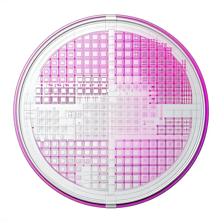
Wafer Map Analysis
Spatial pattern recognition on KLARF defect coordinate data. Edge ring, center spot, arc, scratch, and random — classified at defect densities too low for conventional SPC rule violations to fire.
How the wafer map classifier works.
The wafer map analysis module receives defect coordinate data from KLARF files and bin map exports. It normalizes coordinates to a standard die-grid reference frame, then runs a CNN-based spatial pattern classifier that produces a pattern label, a confidence score, and a set of supporting die coordinates for each wafer.
The classifier distinguishes systematic patterns (edge ring, center spot, arc, scratch) from random defect distributions. Systematic patterns are immediately forwarded to the commonality analysis module for cross-lot equipment attribution. Random distributions are scored against D0 thresholds and trigger yield trend tracking only.
Results are available per-wafer, per-lot, and in fleet-trend aggregations. The output drives the ranked evidence package the yield engineer receives for each excursion event.
| Parameter | Description | Value |
|---|---|---|
| Inference time | Per wafer on NVIDIA A30 | 43 ms |
| Inference time (CPU) | Per wafer on 32-core server | 380 ms |
| Pattern accuracy | 14nm and below, KLA-class inspectors | 97.3% |
| Minimum D0 | Detection threshold (pattern recognizable) | 0.03 defects/cm² |
| Supported formats | KLARF 1.0 / 1.8 / 2.0 + IBIS / HMI CSV | — |
| Wafer diameters | Supported die-grid calibrations | 200mm, 300mm |
Eight spatial pattern classes.
Edge Ring
Circular band of elevated defect density 2–8mm from wafer edge. Indicates edge exclusion zone contamination, bevel particle issues, or chuck contact at the edge ring.
Center Spot
Concentrated defect cluster at wafer center. Characteristic of spin-coat non-uniformity, center-high CMP, or electrostatic discharge events at the chuck center pin.
Scratch / Linear
Linear defect track across the wafer surface. Indicates mechanical contact during handling, wafer transport, or a contaminated robot arm end effector.
Arc / Partial Ring
Partial ring or arc pattern consistent with radial non-uniformity in specific quadrants. Common in etch uniformity outliers or gas flow asymmetry in single-wafer chambers.
Hot Spot / Cluster
Localized cluster not at center or edge, correlated to a specific die-coordinate region. Frequently maps to a mask or reticle field defect recurring across repeated exposure fields.
Random
Spatially uncorrelated defect distribution with no detectable pattern. Classified as random and passed to D0 trend tracking rather than equipment attribution analysis.
From KLARF file to pattern label.
Coordinate Normalization
KLARF defect coordinates converted to die-grid reference frame. Wafer diameter and die layout from lot traveler. Coordinate system aligned across inspection tools.
Density Map Construction
Defect counts binned to a spatial density grid. Kernel density estimation applied for smooth spatial signal. Background D0 baseline subtracted to highlight excursion-specific signal.
CNN Classifier
Density map passed to the trained CNN classifier. Multi-class output: pattern label + confidence score. Low-confidence outputs flagged for yield engineer review rather than auto-attributed.
Attribution Handoff
Systematic pattern: immediately forwarded to commonality analysis module for cross-lot equipment attribution. Random: added to D0 trend. Mixed: both paths run in parallel.
See your wafer maps classified in minutes.
Bring a representative KLARF file set. We'll run the pattern classifier and show you what it finds — edge ring, scratch, or random — in your first session.